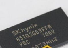
H5TQ2G63FFR-PBC Suited For The Main Memory Applications Which Requires Large Memory Density And High Bandwidth
1.
1.Description
The H5TQ2G83GFR-xxC, H5TQ2G63GFR-xxC,H5TQ2G83GFR-xxI, H5TQ2G63GFR-xxI, H5TQ2G83GFR�xxL,H5TQ2G63GFR-xxL,H5TQ2G83GFR-xxJ,H5TQ2G63GFR-xxJ are a 2,147,483,648-bit CMOS Double Data
Rate III (DDR3) Synchronous DRAM, ideally suited for the main memory applications which requires large
memory density and high bandwidth. SK Hynix 2Gb DDR3 SDRAMs offer fully synchronous operations ref�erenced to both rising and falling edges of the clock. While all addresses and control inputs are latched on
the rising edges of the CK (falling edges of the CK), Data, Data strobes and Write data masks inputs are
sampled on both rising and falling edges of it. The data paths are internally pipelined and 8-bit prefetched
to achieve very high bandwidth.
2.FEATURES
* This product in compliance with the RoHS directive.
• VDD=VDDQ=1.5V +/- 0.075V
• Fully differential clock inputs (CK, CK) operation
• Differential Data Strobe (DQS, DQS)
• On chip DLL align DQ, DQS and DQS transition with CK
transition
• DM masks write data-in at the both rising and falling
edges of the data strobe
• All addresses and control inputs except data,
data strobes and data masks latched on the
rising edges of the clock
• Programmable CAS latency 5, 6, 7, 8, 9, 10, 11, 12, 13
and 14 supported
• Programmable additive latency 0, CL-1, and CL-2
supported
• Programmable CAS Write latency (CWL) = 5, 6, 7, 8
9 and 10
• Programmable burst length 4/8 with both nibble
sequential and interleave mode
• BL switch on the fly
8banks
• Average Refresh Cycle (Tcase 0 oC~ 95 oC)
- 7.8 µs at 0oC ~ 85 oC
- 3.9 µs at 85oC ~ 95 oC
Commercial Temperature( 0oC ~ 95 oC)
Industrial Temperature( -40oC ~ 95 oC)
• JEDEC standard 78ball FBGA(x8), 96ball FBGA(x16)
• Driver strength selected by EMRS
• Dynamic On Die Termination supported
• Asynchronous RESET pin supported
• ZQ calibration supported
• TDQS (Termination Data Strobe) supported (x8 only)
• Write Levelization supported
• 8 bit pre
4.Why choose us?
100% new and originao with Advantage price
High efficiency
Fast Delivery
Professional team service
10 Years Experience Electronic components
Electronic components Agent
Advantage logistic discount
Excellent After-sales Service.
Product Tags:

|
|
128M DRAM 2G Electronic Integrated Circuits H5TQ2G63FFR-PBC Images
|